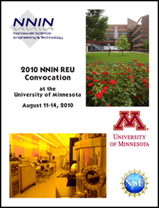
2010 NNIN REU Program
|
|
|
 |
 |
|
The 2010 NNIN REU Convocation Proceedings,
|
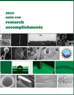
The 2010 NNIN REU Research Accomplishments |
Each link below is to a PDF file, anywhere from 200K to 2.6MB in size.
National Nanotechnology Infrastructure Network Research Experience for Undergraduates (NNIN REU) Program
2010 Research Accomplishments
Table of Contents
Biological Applications, pages 2-39
Characterization of dsDNA Binding Protein SlyA for Nanostructure Assembly, page 2
Kathleen Bennett, Biology, Harvey Mudd College
Measurement and Analysis of Blood Platelet Activation within a Microfluidic Device, page 4
Steven Chase, Biomedical Engineering and Biochemistry and Molecular Biology, Rose-Hulman Institute of Technology
Cytotoxicity of Copper Oxide Nanoparticles and Associated Ions on Human Epithelial Lung Cells (A549), page 6
Sarah Connolly, Microbiology and Cell Science, University of Florida
Characterization of Biomolecular Interactions at the Silicon Photonics Interface, page 8
Lauren Cummings, Chemical Engineering, Oregon State University
Immunomagnetic Detection of Circulating Tumor Cells using a Microfluidic Chip: Cell Recognition and Analysis, page 10
Fraser Downing, Mechanical Engineering, University of Colorado at Boulder
Surface Analysis of DNA Microarrays, page 12
Megan Dunn, Chemical Engineering, University of Arkansas
Electrochemical and Adhesion Properties of PEDOT:PSS as a Coating for Gold Electrodes for Applications in Metal-Molecule-Metal Junctions, page 14
Vivian Feig, Chemical Engineering, Columbia University
Portable Diagnostic System for the Purification and Detection of Biomolecules, page 16
Emily Hoffman, Biomedical Engineering, Case Western Reserve University
Light Dependent Microbial Responses to Cu-doped TiO2 Nanoparticles, page 18
Kristen Jones, Chemistry, Carthage College
Effect of Deposition Characteristics on Electrochemically Prepared PEDOT Films, page 20
Adam Kozak, Biomedical Engineering, University of Rochester
Nanotherapeutics for Advanced Cancer Disease, page 22
Christopher Lowe, Chemical Engineering, University of Massachusetts Amherst
Patterning Neurons with Microcontact Printing on Silicon Oxide Substrates, page 24
Margaret Merritt, Biomedical Engineering, Brown University
High Resolution Surface Plasmon Resonance Microscopy Based Microarray, page 26
Evan Mirts, Biology and Physics, Truman State University
Synthetic Antiferromagnetic Particles for Biosensing, page 28
Kelsey Morse, Chemistry, Beloit College
Plasmonic Nanoparticle Dimer Sensors, page 30
Heidi Nelson, Chemical Engineering, University of Minnesota
Porous Microbeads as Three-Dimensional Scaffolds for Tissue Engineering, page 32
Jennifer Wang, Biomedical Engineering, Duke University
Encapsulation of Single Cells in a Droplet-Based Microfluidic Device, page 34
Yingxia Wang, Chemical Engineering, Massachusetts Institute of Technology
Cell Viability and Morphology on Carbon Nanotube Microstructures, page 36
Masaki Watanabe, Applied Chemistry, Nagoya University
Designing Nano-Engineered Substrates to Probe Cell Organization, Motion and Traction Forces, page 38
Erin Watson, Bioengineering, Rice University
Chemistry, pages 40-53
Design of Organic Conductors Comprised of Fullerene and Lanthanum Triple-Decker Porphyrin Complexes, page 40
Mark Borysiak, Chemical and Biomolecular Engineering, The Ohio State University
Initial Stages of Tantalum Nitride Atomic Layer Deposition, page 42
John Davis, Department of Chemistry, Carleton College
Synthesis and Characterization of Oxide-Embedded and Surface-Passivated Silicon Nanocrystals, page 44
Hiromasa Fujii, Electrical Engineering, University of Tokyo
Characterization of Dynamics of Solvents Encapsulated in Nano-Scale Volumes, by Selective Enhancement of NMR Signal via Dynamic Nuclear Polarization, page 46
Audrey Hammack, Chemistry, The University of Texas at Tyler
Multimodal Optical and MRI Studies with Multifunctional Spinel Nanoparticles, page 48
Chantalle Le, Chemistry, University of California Los Angeles
Surface Treatments to Control the Wettability of Photonic Crystal Bio-Sensors, page 50
Philip Ponce de Leon, Physics and Mechanical Engineering, New York University, The Stevens Institute of Technology
All-Copper Pillar Interconnects, page 52
Barrett Worley, Chemistry, Samford University
Electronics, pages 54-81
Development of Advanced Carbon Electrodes for use in Microfluidic Vanadium Redox Fuel Cells, page 54
Richard Anger, Mechanical Engineering State University of New York at Stony Brook
Ferroelectric Thin Films for Reconfigurable RF Electronics in Next Generation Wireless Communications, page 56
Scott Bakkila, Physics and Computer Science, Lawrence Technological University
Laminated Anodes and Electron Transport Layers in Organic Inverted Bulk Heterojunction Solar Cells, page 58
Lia Bersin, Chemical Engineering, Columbia University
Nanowire Photovoltaics in Photoelectrochemistry and Plasmonic Ring Structures, page 60
Clara Chow, Biomedical Engineering, University of Wisconsin-Madison
Optimization of Ohmic Contacts to III-N Semiconductor Material, page 62
Austin Conner, Electrical Engineering, Vanderbilt University
Heterogeneous Integration of p- and n-type Nanowires for Complementary Nanowire Circuits, page 64
Zachary Henderson, Electrical Engineering, University of Massachusetts Amherst
Fabrication of Magneto Resistance-Based Magnetic Quantum-Dot Cellular Automata, page 66
Angeline Klemm, Physics/Engineering, University of Wisconsin-La Crosse
Semiconductor Nanocrystal Inks for Printed Photovoltaics, page 68
Gabriel Palomino, Chemical Engineering, Texas Tech University
Graphene Contacts to Pentacene Thin-Film Transistors, page 70
Christopher Phare, Physics and Mathematics, Vanderbilt University
Graphene Nanoribbons as Transistors in Nanoelectronic Devices, page 72
Michelle Pillers, Chemistry, Southern Methodist University
Thermally Enhanced Dynamic Core Migration with Phase Change Materials, page 74
Amber Pizzo, Mechanical Engineering, Binghamton University
Fabrication and Characterization of Indium Arsenide Nanowire Transistors, page 76
Devanand Sukhdeo, Electrical Engineering, Columbia University
Heterogeneous Integration of p- and n- type Nanowires for Complementary Nanowire Circuits, page 78
Takeshi Uchinoumi, Chemical Systems and Engineering, Kyushu University
Fabrication of a Gallium Nitride Nano-Field Effect Transistor, page 80
Amber C. Wingfield, Optical Engineering and Mathematics, Norfolk State University
Materials, pages 82-113
Heterojunction Growth of Si1-xGex and C3N4 Nanowires on Silicon, page 82
Siatta Adams, Chemistry, Mercer University
Nanoparticle-Enhanced Tunnel Junctions for High-Efficiency Multi-Junction Solar Cells, page 84
Gavin P. Campbell, Materials Science and Engineering, University of Illinois at Urbana-Champaign
Investigation of the Effects of Base Additives in Molecular Glass Photoresist Films, page 86
Sylvia Carroll, Electrical Engineering and Biology, University of Texas at El Paso
Contact Resistance of Graphene-Based Devices by TLM, page 88
Arolyn Conwill, Physics, Pomona College (undergraduate), Massachusetts Institute of Technology (graduate)
Aluminum Induced Crystallization of Silicon on Quartz for Silicon Wire Array Solar Cells, page 90
Natalie M. Dawley, Physics, University of Virginia
Fabrication of Dendritic Electrodes for Electroactive Polymer Actuators, page 92
Nathaniel Hogrebe, Chemical Engineering, University of Dayton
Grain Boundary Effects on Charge Transport In ZnO:Al Transparent Conducting Films, page 94
Ruby Lee, Bioengineering, Stanford University
Adhesion of Capillary Underfill Epoxies for Flip Chip Packaging, page 96
Gillian Lui, Environmental Studies and Conservation Biology, Middlebury College
Temperature Dependent Growth Properties of Epitaxial Graphene on Carbon-Face Silicon Carbide, page 98
Benjamin D. Mahala, Chemistry, University of Missouri Science and Technology
Composite Cathodes for Intermediate Temperature Solid Oxide Fuel Cells, page 100
Isaac Markus, Chemical Engineering, The Cooper Union for the Advancement of Science and Art
Raman Studies in Graphene, page 102
Nkemdilim Oghedo, Chemical Engineering, Yale University
Characterization of SiAlON for Hydrogen Diffusion Barrier Application in Nonvolatile Memory Devices, page 104
Axel Palmstrom, Chemical Engineering, University of California Santa Barbara
Silicon Phononic Crystals for High Efficiency Thermoelectrics, page 106
Christopher Romanczuk, Chemical and Biomolecular Engineering, Rice University
Characterization of Materials with Epitaxially Embedded Nanoinclusions for Thermoelectric Applications, page 108
Joseph S.T. Smalley, Engineering Science and Mechanics, The Pennsylvania State University
Low Stress Oxides for use in Microfabricated Ion Traps for Quantum Computation, page 110
Margeaux Wallace, Materials Science and Engineering, Cornell University
Solution Synthesis and Aerosol Deposition of Cu2ZnSnS4 Nanoparticles, page 112
Denys Zhuo, Material Science and Engineering, Massachusetts Institute of Technology
Mechanical Devices, pages 114-129
Real Time Blood Coagulation Sensor, page 114
Jennie Appel, Electrical Engineering, Auburn University
Locomotion of Catalytic Nanomotors, page 116
Jesse Ault, Mechanical Engineering, Purdue University
Fabrication of a Three Terminal Nanomechanical Graphene Switch, page 118
Lauren Cantley, Physics, Grinnell College
Mechanics of 1-25 nm Thin Films, page 120
Zachary J. Connell, Mechanical Engineering, University of Nebraska
Top-Down Fabrication of Patterned, Vertically Aligned Silicon Nanowires, page 122
Sibu Kuruvilla, Materials Science and Engineering, University of Illinois at Urbana-Champaign
Ion Distribution in Ionomer and High Temperature Ionic Liquid Actuators, page 124
Stephen Twigg, Department of Electrical Engineering, Villanova University
Micropore Immunosensors for Fast Disease Diagnostics, page 126
Clare Wardwell, Biological Sciences, University of Delaware
Improving Quality Factor of Drum Resonators via Gas Confinement, page 128
Diana Wu, Chemical Engineering and Biology, Massachusetts Institute of Technology
Optics and Opto-Electronics, pages 130-155
Growth of Graphene Nanostructures on Silicon Wafers, page 130
Brian Benton, Physics, University of Minnesota-Twin Cities
Fabrication of Silver MicroWire Polarization Filters, page 132
Diana Bolser, Physics, University of Missouri-Columbia
Automation of Sample-Positioning and Data-Collection for Pulsed-Laser-Melting Experiments, page 134
Edy Cardona, Physics, University of California, Berkeley
Fabrication of High Speed Nanoscale Metal-Semiconductor-Metal Photodetector, page 136
Kevin Chen, Electrical Engineering, Arizona State University
Characterization of Ag-Si Composite for Infrared Photodetectors, page 138
Marie DesHarnais, Civil Engineering, University of Minnesota-Twin Cities
Fabrication of Photonic Crystals for High Temperature Applications, page 140
Joseph DeWilde, Chemical Engineering, Oregon State University
Transfer of Electron Beam-Patterned Photonic Nanobeam Cavities to Flexible Substrates, page 142
D. Johann Djanal-Mann, Electrical Engineering, University of Florida
3D Super-Resolution Using a Phase Mask Fabricated via Grey-Level Lithography, page 144
Callie Fiedler, Physics, University of San Diego
Fabrication and Characterizations of Plasmonic Nanostructures for Organic Photovoltaics, page 146
Michael Hoerner, Engineering Physics, Rose Hulman Institute of Technology
Close-Packed Monolayer of Silica Nanoparticles for use as Etch Mask in LED Active Region, page 148
Christina Jones, Engineering Physics, University of Colorado at Boulder
Molecular Specific Biosensing Based on Engineered Quasi-3D Plasmonic Nanostructures, page 150
Roger Jordan, Biomedical Engineering, Texas A&M University
Lifetime of Charge Carriers in Single Silicon Nanowire, page 152
Jhim Handrex Meza, Electrical Engineering, University of California, Los Angeles
Quantum Well Intermixing on a Hybrid Silicon or Silicon Dioxide Bonded AlGaAs/GaAs/InGaAs Platform, page 154
Mohsin Pasha, Electrical Engineering, University of Texas at Austin
Physics and Nanostructure Physics, pages 156-163
Unipolar Resistive Switching in 100 nm2 Pt-NiO-Ni-Pt Cells, page 156
Matthew T. Hershberger, Physics, Bethel College, Kansas
Tunneling Electron Microscopy Investigation Strategy for InAs Nanowires, page 158
Jacob Alexander Sadie, Electrical Engineering, University of California-Berkeley
Domain Wall Track in a Praseodymium Strontium Manganite Oxide Nanobridge, page 160
Meng Shi, Physics, Case Western Reserve University
Transport Properties of InAs Nanowires for Applications in Quantum Information Processing, page 162
Hamsa Sridhar, Physics and Mathematics, Harvard College
Process and Characterization, pages 164-201
Characterization of Mercury and Copper Capped DMBP Monolayers, page 164
Narahi J. Alvarez, Chemical Engineering Department, University of Puerto Rico-Mayaguez Campus
Process Development for Writing Sub-100 nm Linewidths using a Scanning Electron Microscope, page 166
Hilton H. Augustine III, Electrical Engineering, Harvard University
The Role of Polyvinylpyrrolidone in the Toxicity Evaluation of Silver Nanocubes, page 168
Mark Brunson, Mechanical Engineering, San Francisco State University
Characterization of Ruthenium Electrodes for Implantable Neurostimulation Applications, page 170
Christine Burdett, Chemical Engineering, North Carolina State University
Characterization of Iron Oxide Integration within Phospholipid Encapsulated Colloids, page 172
Jack Chen, Biomedical Engineering, Duke University
Material Characterization of Advanced III-V Semiconductors for Nanophotonic Integration, page 174
Brian T. Chung, Engineering Physics, University of Michigan – Ann Arbor
Fabrication of Locally-Gated Bilayer Graphene Field Effect Transistors, page 176
Corey E. Clapp, Department of Chemistry, Amherst College, Amherst
Graphene Growth on Palladium (111), page 178
Scott Isaacson, Chemical Engineering, University of Minnesota
DNA Electrophoresis in Microfabricated Post Arrays, page 180
Jason Lee, Chemical Engineering, University of Massachusetts-Amherst
Process for Detaching Suspended Graphene Structures from Silicon Carbide, page 182
Charles Mackin, Electrical Engineering, University of Arizona
Sub-20 Nanometer Electron Beam Induced Deposited Gold Plasmonic Nanostructures, page 184
Claire McLellan, Physics, Wake Forest University
Fabrication of Graphene Structures Using an Atomic Force Microscope, page 186
Christopher O'Connell, Mechanical Engineering, University of Rhode Island
Fabrication of Gold Nanoparticles Using E-beam Lithography: Effect of Development Conditions on Shape and Resolution, page 188
Fiona O'Connell, Materials Engineering, Loyola University Maryland
C10- and C12- BTBT Single Crystalline Organic Field Effect Transistor, page 190
Si Hui Athena Pan, Physics, Brandeis University
Transferring Chemical Vapor Deposition Grown Graphene, page 192
Phi Pham, Physics, University of Colorado Boulder
High Spatial Resolution Kelvin Probe Force Microscopy with Shielded Probes, page 194
Kevin J. Satzinger, Physics and Mathematics, Truman State University
Characterization of High Aspect Ratio Silver Micromachining for Radio Frequency Inductors, page 196
Natalie Swider, Material Science and Engineering, University of Illinois Champaign-Urbana
Template Stripping for High Throughput Fabrication of Nanohole Arrays, page 198
Benjamin Treml, Engineering Physics, University of Wisconsin-Madison
Sputtered TiW/W Emitter Contact Stack Design in Terahertz Bipolar Transistors, page 200
Jeremy Wachter, Physics and Electrical Engineering, Rose-Hulman Institute of Technology
Social and Ethical Issues of Nanotechnology, pages 202-205
Public Service Posters for the Societal and Ethical Issues (SEI) of Nanotechnology, page 202
Chloe Lake, Communication and Psychology, University at Buffalo